

- Mark as New
- Bookmark
- Subscribe
- Mute
- Subscribe to RSS Feed
- Permalink
- Report Inappropriate Content
Hi,
I'm trying to use the watermarks to end the GPIF2 data transfers.
My FX3 design is a 32b slave FIFO with flagA as ready/empty and flagB as watermark (both thread dependent). When accessing the FX3 in RD mode (U2P), the watermark is working as expected and everything goes great.
When accessing in WR mode (P2U), for some reason, the watermark comes earlier than what I would expect. I'm sending a whole FX3 buffer (16KB) from my FPGA and counting the amount of data sent (in 32b words), so for now the watermark flag it is not at the FPGA side.
The watermark for P2U access is configured with a value of 6, so, according to the documentation, the flag should go down when there are 2 samples left to be sent. At the FPGA I'm double registering the watermark, so I'm expecting the watermark to become low when there is no more data to be sent. However I still see that, even after the 2 cycle delay, the watermark does not arrive where I am expecting it.
I'm including the chip scope capture so you can have a look, as well.

The configuration for the FX3 watermark is as follows:

Thanks in advance.
Solved! Go to Solution.
- Labels:
-
USB Superspeed Peripherals
- Mark as New
- Bookmark
- Subscribe
- Mute
- Subscribe to RSS Feed
- Permalink
- Report Inappropriate Content
Hello,
Actually it should be at 4093th
>> In the burst mode trace, the flag B (00) is seen on the 4094th edge (i.e. the edge at which cursor is placed), so the actual FLGA B pin would have been driven low by FX3 at 4092 clock edge.
Two words of data need to be written after the clock edge at which Flag B is sample LOW. So, if the actual flag B is going low at 4093th clock edge then only one data word is written (i.e. at 4094 th clock edge) as at 4095 the clock edge the SLWR is de asserted
To know if the data is over sampled at some point or if the problem is from the watermark side. Please follow the watermark flag and stop the data transfers accordingly. The DMA buffer on FX3 will be full and committed to USB. Please check the data received by USB using Control center. Based on the data read we can know if the data sent and received are same. If not, there might be some problem in timings of Slave FIFO write.
As multiple threads for reads and writes are used in your design unlike default AN65974, please let me know if the custom GPIF state machine can be shared.
Rashi
- Mark as New
- Bookmark
- Subscribe
- Mute
- Subscribe to RSS Feed
- Permalink
- Report Inappropriate Content
Hi,
Just to be super clear...when the documentation says:
-
The number of data words that may be written after the clock edge at which the partial flag is sampled low = watermark x (32/bus width) – 4.
In the scenario described above, does it means that when I sample the watermark value and it's 0, I need to stop sending on the next clock cycle (but the current one it is still allowed)????
Thanks

- Mark as New
- Bookmark
- Subscribe
- Mute
- Subscribe to RSS Feed
- Permalink
- Report Inappropriate Content
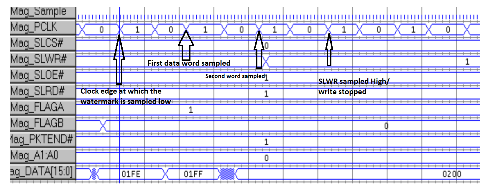
Hello,
As per An65974, the number of data words that may be written after the clock edge at which the partial flag is sampled low = watermark x (32/bus width) – 4.
This means if watermark value is 6 (6* 1 - 4), FX3 will expect 2 data words after the clock edge at which watermark flag is sampled low (attached snippet)
Edited: Please note the attached snippet (example 3 of AN65974) is for 16 bits bus width but the same needs to be implemented when 32 bits bus width is used with watermark value as 6
If the default GPIF state machine is used, the data will be sampled when SLWR is LOW so after the 2 data words are written to FX3 the SLWR should be driven HIGH from the FPGA
Please confirm if writing to FX3 is stopped after writing 2 data words (after the clock edge at which watermark flag is sampled low). The snippet shared by you doesn't include PCLK, please share the snippet with PCLK. Also, the SLWR toggles, please let me know when is the data is sampled at the GPIF SM. Is the implementation same as default GPIF state machine
Please let me know if any queries on this.
Rashi
- Mark as New
- Bookmark
- Subscribe
- Mute
- Subscribe to RSS Feed
- Permalink
- Report Inappropriate Content
Hi,
Regarding the chipscope capture:
- The PCLK clock is the same as the clock I'm sampling with (I can't plot it but every tick is a rising edge of the clock).
- The signals I use internally are active high (it's a design principle I always follow). Then I use an inverter to drive them out. So, if SL_WE is high, it means it's active.
On the other hand, please notice that there are gaps in the burst I'm sending. The controller does not wait for the whole packet to be present and starts sending when a minimum amount of data is present at the input buffer.
While testing this, I've modified the design to always send data, regardless if it's available or not. In this scenario, the watermark flag works as expected (see capture attached).

So my question is: is there anything else I need to take into consideration when working in this mode (non-burst) to use the watermark flags, or it is something not supported by the FX3?
Thanks in advance
- Mark as New
- Bookmark
- Subscribe
- Mute
- Subscribe to RSS Feed
- Permalink
- Report Inappropriate Content
Hello,
In both the traces, I noticed that DMA flags status is like 3,2,0. Can you please explain what does that mean.
At the FPGA I'm double registering the watermark, so I'm expecting the watermark to become low when there is no more data to be sent
>> Please explain this to understand the problem better. From the burst mode trace, the no data is written after Flag B is sampled LOW (00). If the status of the Flag B is buffered twice, the actual Flag B (from Fx3) would have been pulled at 4092th clock edge. Is my understanding correct?
Also, confirm if the address lines (thread address) are not changed in between while write to FX3 is done (i.e. are there any reads in between the writes to FX3). If the address is changed in between, the address to flag latency at start of transfer needs to be considered.
The controller does not wait for the whole packet to be present and starts sending when a minimum amount of data is present at the input buffer.
>> From this do you mean that the FX3 commits partial buffer or is it the FPGA is sending the data available with it (that is why no burst mode)
As multiple threads for reads and writes are used in your design unlike default AN65974, please let me know if the custom GPIF state machine can be shared.
Rashi
- Mark as New
- Bookmark
- Subscribe
- Mute
- Subscribe to RSS Feed
- Permalink
- Report Inappropriate Content
Hi,
As I mentioned, the DMA flags are sampled with a double register line. I've combined both signals (the delayed 1 and 2 cycles) into a bus for simplicity.
At the burst mode with no gaps, the watermark is configured at 6. According to documentation when the watermark goes low, I should have 2 more write accesses left. However I use the double register so when it comes out of it, no more data needs to be sent.
>> If the status of the Flag B is buffered twice, the actual Flag B (from Fx3) would have been pulled at 4092th clock edge. Is my understanding correct?
Actually it should be at 4093th
>> Also, confirm if the address lines (thread address) are not changed in between while write to FX3 is done (i.e. are there any reads in between the writes to FX3). If the address is changed in between, the address to flag latency at start of transfer needs to be considered.
The address is kept at the same thread for the whole time the access is performed.
>> The controller does not wait for the whole packet to be present and starts sending when a minimum amount of data is present at the input buffer. From this do you mean that the FX3 commits partial buffer or is it the FPGA is sending the data available with it (that is why no burst mode)
It's the FPGA. By design it doesn't know how much data is available at the input buffer. The design defines a minimum packet size that will trigger the GPIF2 WR access (FPGA to FX3), but the real packet size is embedded within the packet and it's caught while transmitting the data. At some point, the data source can't keep up with the GPIF2 bus and gaps in the WR access are introduced.
Best
- Mark as New
- Bookmark
- Subscribe
- Mute
- Subscribe to RSS Feed
- Permalink
- Report Inappropriate Content
Hello,
Actually it should be at 4093th
>> In the burst mode trace, the flag B (00) is seen on the 4094th edge (i.e. the edge at which cursor is placed), so the actual FLGA B pin would have been driven low by FX3 at 4092 clock edge.
Two words of data need to be written after the clock edge at which Flag B is sample LOW. So, if the actual flag B is going low at 4093th clock edge then only one data word is written (i.e. at 4094 th clock edge) as at 4095 the clock edge the SLWR is de asserted
To know if the data is over sampled at some point or if the problem is from the watermark side. Please follow the watermark flag and stop the data transfers accordingly. The DMA buffer on FX3 will be full and committed to USB. Please check the data received by USB using Control center. Based on the data read we can know if the data sent and received are same. If not, there might be some problem in timings of Slave FIFO write.
As multiple threads for reads and writes are used in your design unlike default AN65974, please let me know if the custom GPIF state machine can be shared.
Rashi