

- Mark as New
- Bookmark
- Subscribe
- Mute
- Subscribe to RSS Feed
- Permalink
- Report Inappropriate Content
Hi,
to reduce the resource requirements of my design I consider the use of DP. I wrote the FSM in pure verilog without DP components and the PSoC is up to 98% full.
Anyway, the idea is to load a timer by using a verilog hardware period register (which is written by another verilog instance). The common approch of the DP Video Tutorials AN 21{1-4} is to use CPU registers to load the period into e.g. D1 or even F1. Now I need to load it from PI port of cy_psoc3_dp (which offers the possibility to do this). But I can't use it for comparision usage since the condition signals generator by the DP is limited to the internal registers A{0,1} or D{0,1}. Further more it seems that I can't load the external register value to a fifo register Fx and than load it to an Dx register since there is no parallel port in.
To be short: How can I configure the DP for an external period register - e.g. the 16-bit PWM example with verilog limit and period register?
Thanks
- Labels:
-
PSoC 5LP

- Mark as New
- Bookmark
- Subscribe
- Mute
- Subscribe to RSS Feed
- Permalink
- Report Inappropriate Content
- Mark as New
- Bookmark
- Subscribe
- Mute
- Subscribe to RSS Feed
- Permalink
- Report Inappropriate Content
oops, I miss the edit button. Anyway.
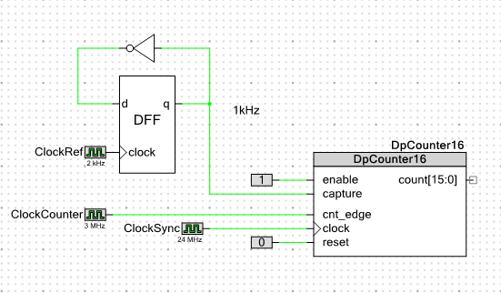
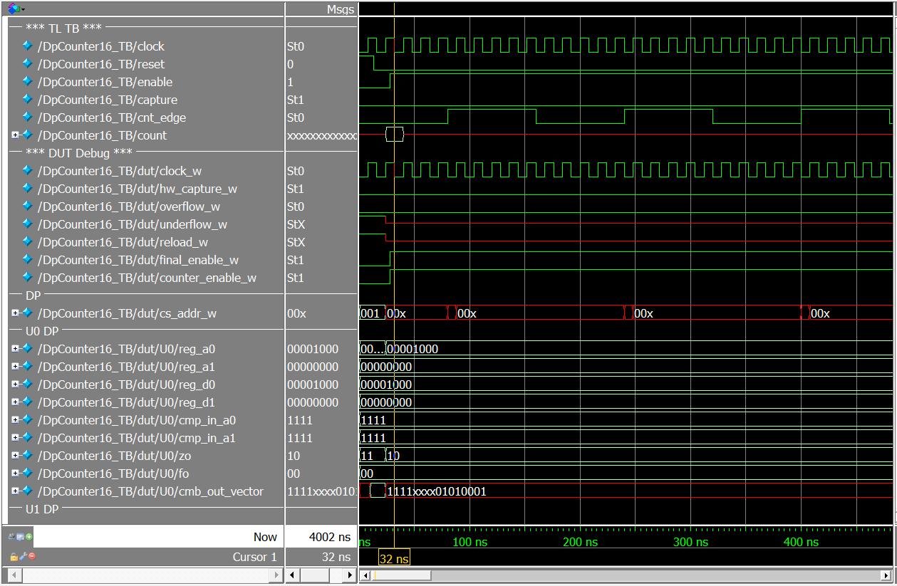
The first shoot above shows the Symbol I want to implement using DP (with Testbench). The goal is to have the count value on port; not at any CPU register. These pic attached below show the Modelsim simulatiom. The problem is the wrong 'unspecified' signals of ff0 and z0. Due to this the cs_addr get wrong the whole design can't work. Any ideas what gone wrong? Maybe/Probably I misconfigured the DP ? Are there rule of thumb to debug DP elements? I use the presynthesis DP implementation here.
assign cs_addr_w[2:0] = { 1'b0, count_enable_w, reload_w };
parameter dpconfig0 =
{
`CS_ALU_OP_PASS, `CS_SRCA_A0, `CS_SRCB_D0,
`CS_SHFT_OP_PASS, `CS_A0_SRC_NONE, `CS_A1_SRC_NONE,
`CS_FEEDBACK_DSBL, `CS_CI_SEL_CFGA, `CS_SI_SEL_CFGA,
`CS_CMP_SEL_CFGA, /*CFGRAM0: Idle*/
`CS_ALU_OP_PASS, `CS_SRCA_A0, `CS_SRCB_D0,
`CS_SHFT_OP_PASS, `CS_A0_SRC___D0, `CS_A1_SRC_NONE,
`CS_FEEDBACK_DSBL, `CS_CI_SEL_CFGA, `CS_SI_SEL_CFGA,
`CS_CMP_SEL_CFGA, /*CFGRAM1: Reload Period (A0 <= D0)*/
`CS_ALU_OP__INC, `CS_SRCA_A0, `CS_SRCB_D0,
`CS_SHFT_OP_PASS, `CS_A0_SRC__ALU, `CS_A1_SRC_NONE,
`CS_FEEDBACK_DSBL, `CS_CI_SEL_CFGA, `CS_SI_SEL_CFGA,
`CS_CMP_SEL_CFGA, /*CFGRAM2: Increment A0 (A0 <=A0 + 1)*/
`CS_ALU_OP_PASS, `CS_SRCA_A0, `CS_SRCB_D0,
`CS_SHFT_OP_PASS, `CS_A0_SRC_NONE, `CS_A1_SRC_NONE,
`CS_FEEDBACK_DSBL, `CS_CI_SEL_CFGA, `CS_SI_SEL_CFGA,
`CS_CMP_SEL_CFGA, /*CFGRAM3: UNUSED*/
`CS_ALU_OP_PASS, `CS_SRCA_A0, `CS_SRCB_D0,
`CS_SHFT_OP_PASS, `CS_A0_SRC_NONE, `CS_A1_SRC_NONE,
`CS_FEEDBACK_DSBL, `CS_CI_SEL_CFGA, `CS_SI_SEL_CFGA,
`CS_CMP_SEL_CFGA, /*CFGRAM4: UNUSED*/
`CS_ALU_OP_PASS, `CS_SRCA_A0, `CS_SRCB_D0,
`CS_SHFT_OP_PASS, `CS_A0_SRC_NONE, `CS_A1_SRC_NONE,
`CS_FEEDBACK_DSBL, `CS_CI_SEL_CFGA, `CS_SI_SEL_CFGA,
`CS_CMP_SEL_CFGA, /*CFGRAM5: UNUSED*/
`CS_ALU_OP_PASS, `CS_SRCA_A0, `CS_SRCB_D0,
`CS_SHFT_OP_PASS, `CS_A0_SRC_NONE, `CS_A1_SRC_NONE,
`CS_FEEDBACK_DSBL, `CS_CI_SEL_CFGA, `CS_SI_SEL_CFGA,
`CS_CMP_SEL_CFGA, /*CFGRAM6: UNUSED*/
`CS_ALU_OP_PASS, `CS_SRCA_A0, `CS_SRCB_D0,
`CS_SHFT_OP_PASS, `CS_A0_SRC_NONE, `CS_A1_SRC_NONE,
`CS_FEEDBACK_DSBL, `CS_CI_SEL_CFGA, `CS_SI_SEL_CFGA,
`CS_CMP_SEL_CFGA, /*CFGRAM7: UNUSED*/
8'hFF, 8'h00, /*CFG9: */
8'hFF, 8'hFF, /*CFG11-10: */
`SC_CMPB_A1_D1, `SC_CMPA_A1_D1, `SC_CI_B_ARITH,
`SC_CI_A_ARITH, `SC_C1_MASK_DSBL, `SC_C0_MASK_DSBL,
`SC_A_MASK_DSBL, `SC_DEF_SI_0, `SC_SI_B_DEFSI,
`SC_SI_A_DEFSI, /*CFG13-12: */
`SC_A0_SRC_ACC, `SC_SHIFT_SL, 1'h0,
1'h0, `SC_FIFO1_BUS, `SC_FIFO0_BUS,
`SC_MSB_DSBL, `SC_MSB_BIT0, `SC_MSB_NOCHN,
`SC_FB_NOCHN, `SC_CMP1_NOCHN,
`SC_CMP0_NOCHN, /*CFG15-14: */
10'h00, `SC_FIFO_CLK__DP,`SC_FIFO_CAP_AX,
`SC_FIFO_LEVEL,`SC_FIFO__SYNC,`SC_EXTCRC_DSBL,
`SC_WRK16CAT_DSBL /*CFG17-16: */
};
cy_psoc3_dp #(
.a0_init(00),
.a1_init(00),
.d0_init(08),
.d1_init(00),
.cy_dpconfig(dpconfig0))
U0(
/* input */ .reset(reset),
/* input */ .clk(clock_w),
/* input [02:00] */ .cs_addr(cs_addr_w),
/* input */ .route_si(1'b0),
/* input */ .route_ci(1'b0),
/* input */ .f0_load(1'b0),
/* input */ .f1_load(1'b0),
/* input */ .d0_load(1'b0),
/* input */ .d1_load(1'b0),
/* output */ .ce0(),
/* output */ .cl0(),
/* output */ .z0(dp_z0_w),
/* output */ .ff0(dp_ff0_w),
/* output */ .ce1(),
/* output */ .cl1(),
/* output */ .z1(),
/* output */ .ff1(),
/* output */ .ov_msb(),
/* output */ .co_msb(),
/* output */ .cmsb(),
/* output */ .so(),
/* output */ .f0_bus_stat(),
/* output */ .f0_blk_stat(),
/* output */ .f1_bus_stat(),
/* output */ .f1_blk_stat(),
/* input */ .ci(1'b0), // Carry in from previous stage
/* output */ .co(dp_co_w), // Carry out to next stage
/* input */ .sir(1'b0), // Shift in from right side
/* output */ .sor(), // Shift out to right side
/* input */ .sil(1'b0), // Shift in from left side
/* output */ .sol(), // Shift out to left side
/* input */ .msbi(1'b0), // MSB chain in
/* output */ .msbo(), // MSB chain out
/* input [01:00] */ .cei(2'b0), // Compare equal in from prev stage
/* output [01:00] */ .ceo(), // Compare equal out to next stage
/* input [01:00] */ .cli(2'b0), // Compare less than in from prv stage
/* output [01:00] */ .clo(), // Compare less than out to next stage
/* input [01:00] */ .zi(2'b0), // Zero detect in from previous stage
/* output [01:00] */ .zo(), // Zero detect out to next stage
/* input [01:00] */ .fi(2'b0), // 0xFF detect in from previous stage
/* output [01:00] */ .fo(), // 0xFF detect out to next stage
/* input [01:00] */ .capi(2'b0), // Software capture from previous stage
/* output [01:00] */ .capo(), // Software capture to next stage
/* input */ .cfbi(1'b0), // CRC Feedback in from previous stage
/* output */ .cfbo(), // CRC Feedback out to next stage
/* input [07:00] */ .pi(8'b0), // Parallel data port
/* output [07:00] */ .po(dp_po_lsb_w) // Parallel data port
);
- Mark as New
- Bookmark
- Subscribe
- Mute
- Subscribe to RSS Feed
- Permalink
- Report Inappropriate Content
MSB of cs_addr was wrong ...