

- Mark as New
- Bookmark
- Subscribe
- Mute
- Subscribe to RSS Feed
- Permalink
- Report Inappropriate Content
Hi,
I my application I am using a piezo element as a microphone.
I need to amlify and process it but I have 2 problems:
1. How to make a charge mode amplifier using an internal Op-amp (single supply ).
2. How to interface the mic with the chip.
Please help...
Anna
Solved! Go to Solution.
- Labels:
-
PSoC 3
- Mark as New
- Bookmark
- Subscribe
- Mute
- Subscribe to RSS Feed
- Permalink
- Report Inappropriate Content
- Mark as New
- Bookmark
- Subscribe
- Mute
- Subscribe to RSS Feed
- Permalink
- Report Inappropriate Content
If you google something like "single supply opamp microphone circuits" you get
quite a few hits.
One collection of circuits - www.circuitlab.com/browse/by-tag/microphone/
Regards, Dana.
- Mark as New
- Bookmark
- Subscribe
- Mute
- Subscribe to RSS Feed
- Permalink
- Report Inappropriate Content
- Mark as New
- Bookmark
- Subscribe
- Mute
- Subscribe to RSS Feed
- Permalink
- Report Inappropriate Content
Hi Dana!
Thanks for your speed response!
You are great! Youa are answering all the post 🙂 thanks!
I had look on the links but there is 2 problems :
1. I need a charge amplifier - I am continue googling for a single supply one.
2. The signal I want to interface is -Vdd to +Vdd ( AC audio sound) but as I understood the Psoc can only get positiv values. How to overcome the problem?
Thanks again!

- Mark as New
- Bookmark
- Subscribe
- Mute
- Subscribe to RSS Feed
- Permalink
- Report Inappropriate Content
1. I need a charge amplifier - I am continue googling for a single supply one.
The TI ap note shows a charge amp.
2. The signal I want to interface is -Vdd to +Vdd ( AC audio sound) but as I understood the Psoc can only get positiv values. How to overcome the problem?
Capacitively couple it out to external sink ?
Regards, Dana.
- Mark as New
- Bookmark
- Subscribe
- Mute
- Subscribe to RSS Feed
- Permalink
- Report Inappropriate Content
Thanks,
Sorry but I dont understand what does it mean: Capacitively couple it out to external sink ?
Is there any technique to capture ac signal/audio with the psoc?
- Mark as New
- Bookmark
- Subscribe
- Mute
- Subscribe to RSS Feed
- Permalink
- Report Inappropriate Content
I thought you were trying to send audio out as well.
To interface an ac signal to psoc you can simply bias up an opamp to
Vdd / 2. Or dc couple with a pair of Rs to offset input to opamp. Some
techniques -
www.dropbox.com/s/k1yn4m7heaixvmg/ADinput%20negative%20inputs.zip
Here is a techniqe used for biasing up input to A/D -
Note the 100K sets input Z. Larger values can be used but then you should calc offset
due to leakage that will occur, in order to keep track of allowable input CM range.
Regards, Dana.
- Mark as New
- Bookmark
- Subscribe
- Mute
- Subscribe to RSS Feed
- Permalink
- Report Inappropriate Content
Note this technique of offsetting with R to Vdd allows
for - input signals and biasing up to Vdd / 2 for max input
CM range. Also eliminates expensive coupling cap if doing
an AC coupled design. Use the Excel calculator in zip file
I posted to determine R values. One negative is input Z be-
comes the sum of the two Rs used for offsetting.

Regards, Dana.
- Mark as New
- Bookmark
- Subscribe
- Mute
- Subscribe to RSS Feed
- Permalink
- Report Inappropriate Content
Dana thank you very much!
I am going to try!
Thanks!
- Mark as New
- Bookmark
- Subscribe
- Mute
- Subscribe to RSS Feed
- Permalink
- Report Inappropriate Content
You are always welcome !
Dana.
- Mark as New
- Bookmark
- Subscribe
- Mute
- Subscribe to RSS Feed
- Permalink
- Report Inappropriate Content
- Mark as New
- Bookmark
- Subscribe
- Mute
- Subscribe to RSS Feed
- Permalink
- Report Inappropriate Content
If your input signal is .3 to 10 V you do not need any offset as
you have no negative input V. Rather you need to scale as
follows
Vdda >= Vxinput >= 0
So simply use a resistive divider, approximately equal value Rs
if your Vdda is 5V. Note in your case since Vxin is large no need
for PGA, input scaled value right into A/D or an OpAmp buffer.
or is the input signal -.6V to + 1.5V ?
Regards, Dana.
- Mark as New
- Bookmark
- Subscribe
- Mute
- Subscribe to RSS Feed
- Permalink
- Report Inappropriate Content
Here is what I got for range in of -.6 to + 1.5, I translated that
to 0 to + 2.1 V into PSOC. I assumed Vdda of + 5V, and used
it as a reference. Note also if you use the internal Vref you have
to buffer it with a OpAmp follower out to pin, it has very low drive
capability, in the uA range.
Regards, Dana.
- Mark as New
- Bookmark
- Subscribe
- Mute
- Subscribe to RSS Feed
- Permalink
- Report Inappropriate Content
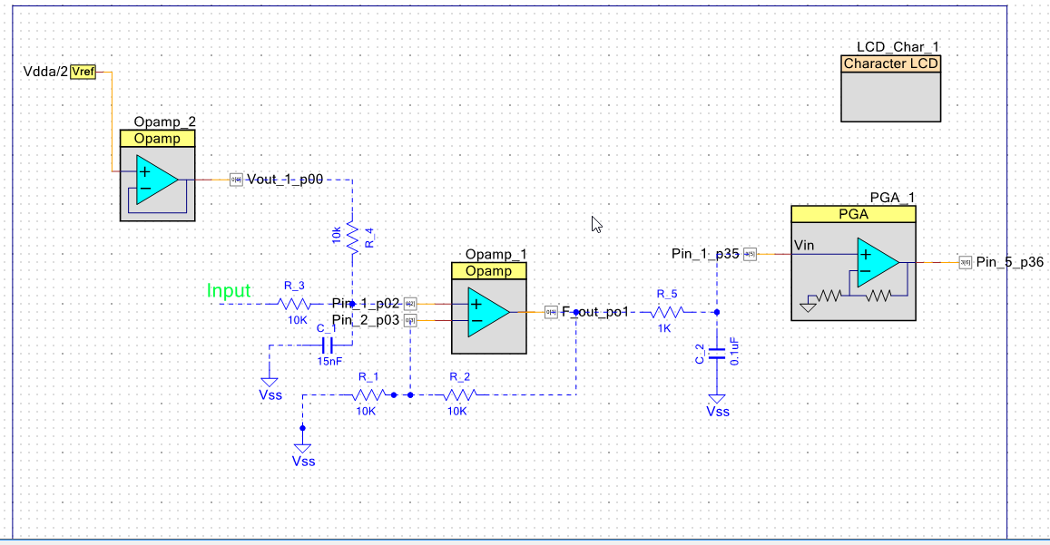
Dana Hi,
I don`t have anought words to express my apreciation for your help!
I made this circuit - pic attached
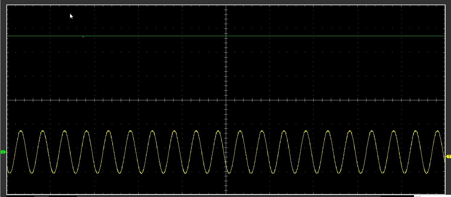
And no metter I do I am getting vary strange results:
-DC Voltage on the PGA output with some noise ( I think so, because my input is 400Hz and the some strange peaks on the output 60-70 KHz) if I put the osilloscope to 500mV range.
-some strange wave if I put the osilloscope to 1V range with the same noise
What I am doing wrong?
- Mark as New
- Bookmark
- Subscribe
- Mute
- Subscribe to RSS Feed
- Permalink
- Report Inappropriate Content
- Mark as New
- Bookmark
- Subscribe
- Mute
- Subscribe to RSS Feed
- Permalink
- Report Inappropriate Content
- Mark as New
- Bookmark
- Subscribe
- Mute
- Subscribe to RSS Feed
- Permalink
- Report Inappropriate Content
And now I have put zero signal on the input and still get the strange wave on the PGA output.
It is no influenced fron the input...
- Mark as New
- Bookmark
- Subscribe
- Mute
- Subscribe to RSS Feed
- Permalink
- Report Inappropriate Content
OpAmp1 is biased, with no input, to Vdd / 2, so that DC voltage is being passed to
the PGA, and assuming its has a G = 2 then its DC no signal output to the pin
will be 5V, at the rail.
Take all your gain in OpAmp 1 and use a OpAmp buffer in place of PGA1 to buffer your LPF.
The input to R3 is DC coupled, I would think you want that AC coupled, otherwise it
affects the bias point for OpAmp1. Lastly make R4 100K and eliminate R3 and C1,
so sigin > Cap > OpAmp1 NI input. Let your filter out of OpAmp1 take care of all the LPF
needs.
Regards, Dana.
- Mark as New
- Bookmark
- Subscribe
- Mute
- Subscribe to RSS Feed
- Permalink
- Report Inappropriate Content
Thanks!!!!
OpAmp1 is biased, with no input, to Vdd / 2, so that DC voltage is being passed to
the PGA - why it is needed Vdd/2 input? in which input?
Take all your gain in OpAmp 1 and use a OpAmp buffer in place of PGA1 to buffer your LPF. - Sorry but didn't understood
Lastly make R4 100K and eliminate R3 and C1, - I have a piezo on the input ( 1Mohm resistance and ~ 47nF capacitance) it will no effect the input of the Opapm? without R3?
so sigin > Cap > OpAmp1 NI input. let your filter out of OpAmp1 take care of all the LPF
needs.
Made the changes as I understood - going to check it....
now it`s right?
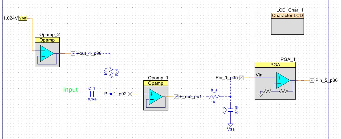
- Mark as New
- Bookmark
- Subscribe
- Mute
- Subscribe to RSS Feed
- Permalink
- Report Inappropriate Content
- Mark as New
- Bookmark
- Subscribe
- Mute
- Subscribe to RSS Feed
- Permalink
- Report Inappropriate Content
I think you need to swap positions of PGA1 and OpAmp1. Take
your G right after input. Note when you setup PGA1 bias its value
needs to be Vdd / 2 / (G + 1) as you want its output to be at Vdd / 2
with no signal in. Voutpga1nosignal = [ Vdd / 2 / (G+1) ] * (G + 1) =
Vdd / 2
So you would have Sigin > PGA 1 > output filterpin > LPF > Input pin > OpAmp1 > output pin
And of course the bias stuff feeding PGA1 input.
Right now you are DC coupled OpAmp 1 into PGA1 so PGA1 Voutnosignal =
Vdd / 2 then that times PGA1 G means its output pegged to rail.
Regards, Dana.
- Mark as New
- Bookmark
- Subscribe
- Mute
- Subscribe to RSS Feed
- Permalink
- Report Inappropriate Content
Hi,
what can cause the PGA not to amlify and have a 2.45V max?
Thanks
- Mark as New
- Bookmark
- Subscribe
- Mute
- Subscribe to RSS Feed
- Permalink
- Report Inappropriate Content
Post your project so forum can take a look at it.
“File” Creator
“Create Workspace Bundle”
Regards, Dana.
- Mark as New
- Bookmark
- Subscribe
- Mute
- Subscribe to RSS Feed
- Permalink
- Report Inappropriate Content
Ok, Thanks!
But why my PGA out is limited to Vdd/2?
I cannot get output more then Vdd/2?
I want my output to be 0-5V aroud Vdd/2 as a trace/offset zero is it possible?
I have eliminated Opamp1 and connected the signal (baised to Vref) directly to the PGA
but the output is cliped on 2.45V.
- Mark as New
- Bookmark
- Subscribe
- Mute
- Subscribe to RSS Feed
- Permalink
- Report Inappropriate Content
Something like this -
- Mark as New
- Bookmark
- Subscribe
- Mute
- Subscribe to RSS Feed
- Permalink
- Report Inappropriate Content
- Mark as New
- Bookmark
- Subscribe
- Mute
- Subscribe to RSS Feed
- Permalink
- Report Inappropriate Content
Another possibility you could try -
- Mark as New
- Bookmark
- Subscribe
- Mute
- Subscribe to RSS Feed
- Permalink
- Report Inappropriate Content
Thanks triyng
R4 is 3.3Mega?
Sorry but maybe I dont understand properly what does it mean: PGA1 biased to Vdd/2?
there is some option to choose?
I chose HighPower
- Mark as New
- Bookmark
- Subscribe
- Mute
- Subscribe to RSS Feed
- Permalink
- Report Inappropriate Content
You want the pga, for no signal in, to have its output biased up
to Vdd / 2 so that you can get maximum dynamic range and lowest
distortion. So you set the input at a DC voltage that causes the output
after gain to be Vdd / 2, with no other signal in.
Its not a setting, its done with the R network that develops the voltage.
3.3M is 3,300,000 ohms.
Regards, Dana.
- Mark as New
- Bookmark
- Subscribe
- Mute
- Subscribe to RSS Feed
- Permalink
- Report Inappropriate Content
Ok
Thanks!
Because only you answer this forum ,
I cann`t afford to continue waste your time and abuse you great help you took to me !
I will "play" with the model so more time, and will post the right circuit that works for the piezo 🙂
Thanks a lot again!
Anna
- Mark as New
- Bookmark
- Subscribe
- Mute
- Subscribe to RSS Feed
- Permalink
- Report Inappropriate Content
I do not think I have a Piezo, but will look for one and try out
the ideas we discussed.
Regards, Dana.
- Mark as New
- Bookmark
- Subscribe
- Mute
- Subscribe to RSS Feed
- Permalink
- Report Inappropriate Content
My errors in the prior circuit recomendations are largely due to the
required HiZ load need by Piezo, so ignore those recomendations.
Here is useful info on characteristics and possible circuits.
http://electronics.stackexchange.com/questions/11187/amplifying-sound-from-a-microphone
https://www.google.com/search?q=piezo+micophone+specs&ie=utf-8&oe=utf-8
Here is calc for biasing the PGA to Vdd / 2
www.daycounter.com/Calculators/Op-Amp/Op-Amp-Voltage-Calculator.phtml
So circuit would look like this -
Note this accomplishes both the biasing and meeting a Zload for Piezo of 10M.
Regards, Dana.
- Mark as New
- Bookmark
- Subscribe
- Mute
- Subscribe to RSS Feed
- Permalink
- Report Inappropriate Content
Here is a working example (WaveDAC simulated Piezo output, 1 Khz ) -
- Mark as New
- Bookmark
- Subscribe
- Mute
- Subscribe to RSS Feed
- Permalink
- Report Inappropriate Content
Hi Dana!
You are great!!!
Thanks a lot!!!
Now I will try it with the real piezo 🙂
I didn`t know that the DAC can simulate wave :))
thanks again!!
- Mark as New
- Bookmark
- Subscribe
- Mute
- Subscribe to RSS Feed
- Permalink
- Report Inappropriate Content
Be aware when you place a scope probe on input to PGA you
will be dropping Zin for the Piezo. Maybe connect a follower to the
Piezo input pin and look at its output to avoid the loading.
One issue I did not look at is the PGA has leakage current on its inputs,
which in turn would cause an offset to be devolped thru the 10M R. So calc
that worst case, chip at elevated temp would be owrst case.
Regards, Dana.
- Mark as New
- Bookmark
- Subscribe
- Mute
- Subscribe to RSS Feed
- Permalink
- Report Inappropriate Content
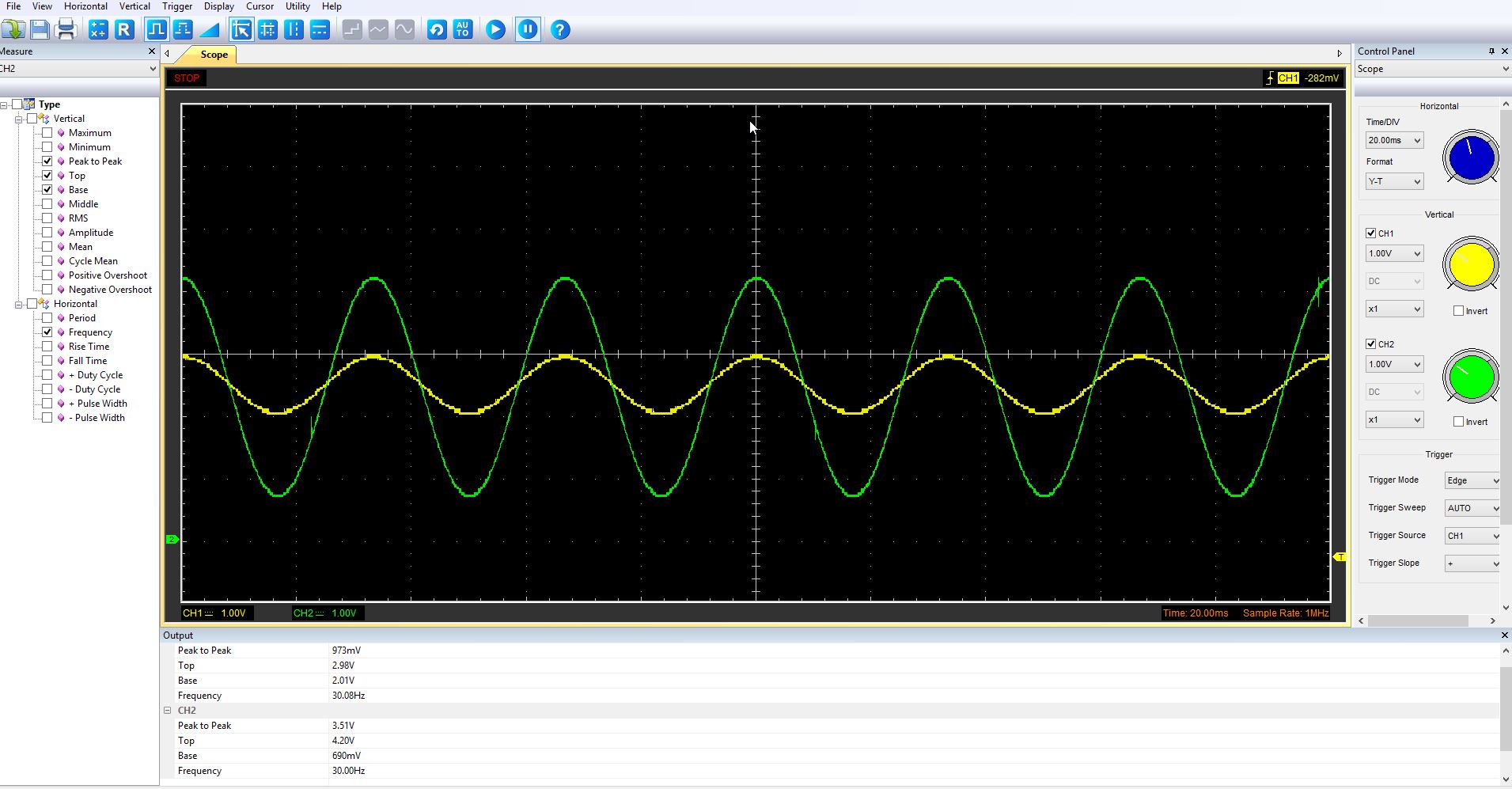
Hi Dear Dana,
I triyed this circuit but there is some problem ... 😞
The same problem I canot overcome for a week
In this way it biased it works great for the inner signal for simulation.
As I input external signal , because the offset is only 0.15 there is values that remain negative and comes zero
the problem is that the offset is gained with all the signal and for big gane and even small signal I am out of the working range
Anna
- Mark as New
- Bookmark
- Subscribe
- Mute
- Subscribe to RSS Feed
- Permalink
- Report Inappropriate Content
Can you post a pic of the input signal and its ground ref, or just a crude
drawing will do.
Are you ac coupled into the input ? I had mentioned earlier input cap not needed
because I thought Piezo looked capacitive, maybe its leakage a problem here so
cap needed ? Not sure.
Note, because the input signal is at bias point of 150 mV that means, DC coupled, that
signal can never be greater that 300 mV pk-pk.
Regards, Dana.
- Mark as New
- Bookmark
- Subscribe
- Mute
- Subscribe to RSS Feed
- Permalink
- Report Inappropriate Content
- Mark as New
- Bookmark
- Subscribe
- Mute
- Subscribe to RSS Feed
- Permalink
- Report Inappropriate Content
- Mark as New
- Bookmark
- Subscribe
- Mute
- Subscribe to RSS Feed
- Permalink
- Report Inappropriate Content
You have the input biased to 2.5V due to the divider, the G = 4 ( 1 + R4 / R6),
so output would = 10V, something does not look right ? Also
loading the Piezo with 10K, much too low....?
Curious, what are you using for a scope ?
Regards, Dana.