Non Volatile RAM (F-RAM & NVSRAM) Forum Discussions
HI,
I am using CY15B064Q-SXE IC as it suits my requirement.
In the product spec it was written that minimum operating temperature is -40 deg.
But in datasheet it is mentioned that, the operating temperature range when powered up is (-50 deg).
Which temperature should i consider.
What is the difference between them.
Thanks & Regards
Naresh
Show Less
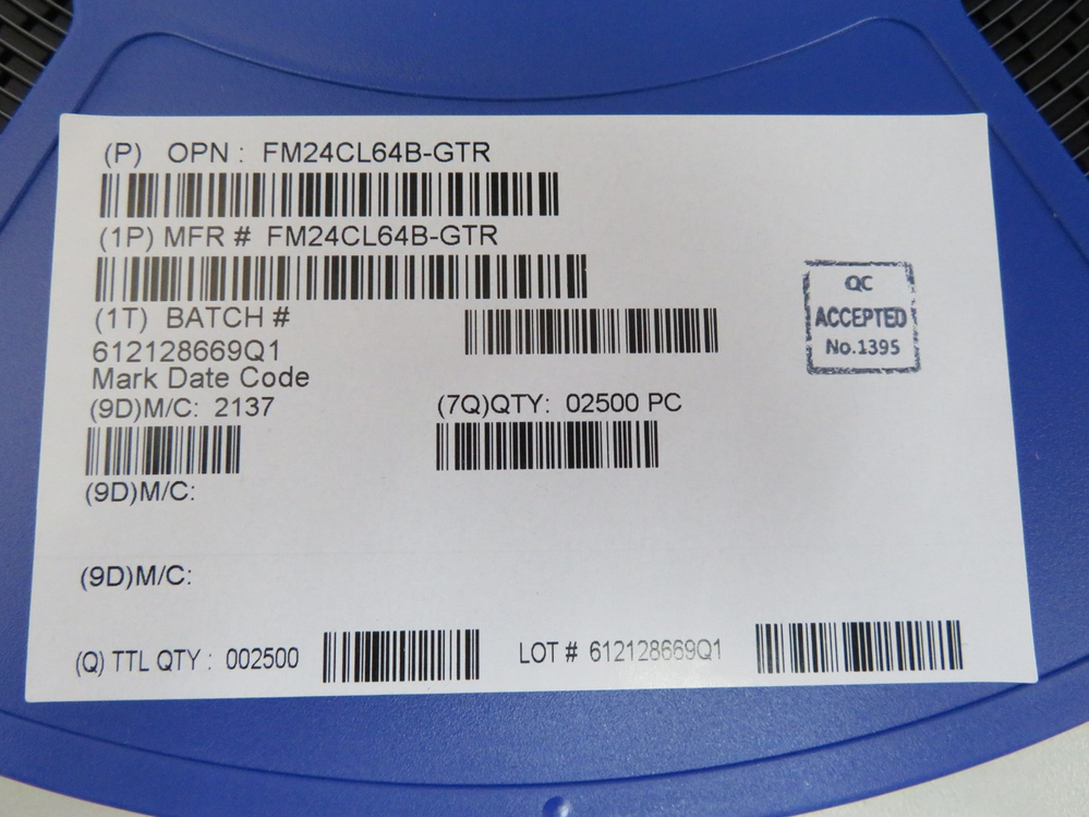
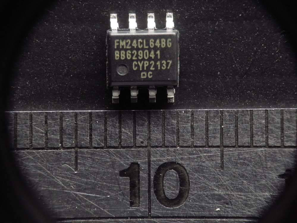
We would like to have your help here. About FM24CL64B-G :
Per the data sheet mentioned the second line of the top marking were BE part Rev code + lot#. But the parts arrived can ‘t match up.
We attached the top marking + datasheet marking + factory label ‘s images for your reference.


Is there any SPI nvSRAM(EEPROM) to support Automotive Grade(-40℃ - 125℃)
I searched in Product Selector Guide website, but not found.
Need your confirmation, thanks
Show LessI am currently using a Cyprus CY14B101I in one of our product lines. This has an i2c bus interface and provides 128K bytes of storage.
I am looking for a larger storage option ideally 512K Bytes and found your FRAM pages mention larger storage option for i2c, SPI and QSPI. But when I go into product selection I can't see any devices which provide an i2c interface, only SPI.
Please advise if you have any i2c storage options for 256K Bytes or larger.
Thanks
Show LessI am designing with the CY14V104NA-BA45XIT. I don't see any guidance in the datasheets of app notes about power sequencing. Is there any requirement for enabling and disabling VCC and VCCQ in relation to each other?
Show LessWhat is the maximum allowable continuous power that CY14B256LA-SZ25XIT can dissipate in a 85 deg C ambient.
The MCU I use is stm32L476RG.
The test steps are as follows:
1. Put FRAM into hibernation mode,
2. Read the FRAM status register and read the value 0x00, indicating that FRAM has entered the hibernate state.
3. Put the MCU into hibernation mode,
4. Wake up MCU after 1 second,
4. Read the FRAM status register, and read the return value 0x40.
The problem is that I shouldn't be able to read the FRAM data at this point because it's still in hibernation mode and I haven't woken it up. I did not find that the CS PIN was pulled down for more than 4.5ms through the logic analyzer.
Show LessHi,
I would like to ask about replacing SRAM 55ns speed grade by 45ns speed grade as I want the feature of non-volatile but the old SRAM in my board using 55ns So not sure I can replace this or not
Show LessDoes anyone have radiation test data on FRAM CY15B102Q (e.g. full part number CY15B102Q-SXM or similar) or on this part family? Looking for gamma “total irradiation dose (TID)” or “single event effects (SEE)”/heavy ion test results.
Hei,
we are using the FM25C160B-G in our desisgns now, but this one is hard to get. Is it possible to use the FM25V02 family for this one, or do you have other alternatives?
Kind regards,
Show Less