

- Mark as New
- Bookmark
- Subscribe
- Mute
- Subscribe to RSS Feed
- Permalink
- Report Inappropriate Content
I have a situation where I am trying to clock out an exact number of pulses from a design-wide clock to an I/O pin. (this is part of a hardware SWD block I'm designing.) I am selecting the desired I/O pin with a demultiplexer and my first idea was to use a UDBClkEn block with a counter to gate the design-wide clock resource out to the physical pin.
Unfortunately this does not work, because the UDBClkEn block can only drive UDB clock input nets and since I am driving an I/O pin through a demux this obviously won't work.
I could drive a D FF but the output clock would be 1/2 of the desired clock. I could create a clock that is 2x the frequency of the design-wide clock but then I'm not guaranteed that it's synchronous. I could use a DDR block but PSoC doesn't have DDR primitives. I could just use an AND gate to gate the clock but now I have to worry about runt pulses.
What is the correct way to route a specific number of clock pulses from a design-wide clock resource through an I/O pin?
- Mark as New
- Bookmark
- Subscribe
- Mute
- Subscribe to RSS Feed
- Permalink
- Report Inappropriate Content
If timing is crucial Verilog solution would of course effect this easily.
If timing not that critical nothing more than a one shot timer counting out
n timing cycles and driving a gate/FF would suffice.
Regards, Dana.

- Mark as New
- Bookmark
- Subscribe
- Mute
- Subscribe to RSS Feed
- Permalink
- Report Inappropriate Content
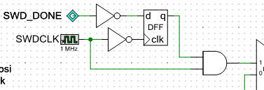
the design-wide clock I'm trying to get out of the device is used internally to synchronize data coming in to the device that is being clocked by that same clock.
I ended up with a negative-edge-triggered FF to create a glitch-free clock enable. I haven't tested it yet:
SWD_DONE goes high when 46 clock cycles have elapsed and stays high until the counter is reloaded. I use a negative edge triggered flip flop to ensure the first rising edge is seen.