

- Mark as New
- Bookmark
- Subscribe
- Mute
- Subscribe to RSS Feed
- Permalink
- Report Inappropriate Content
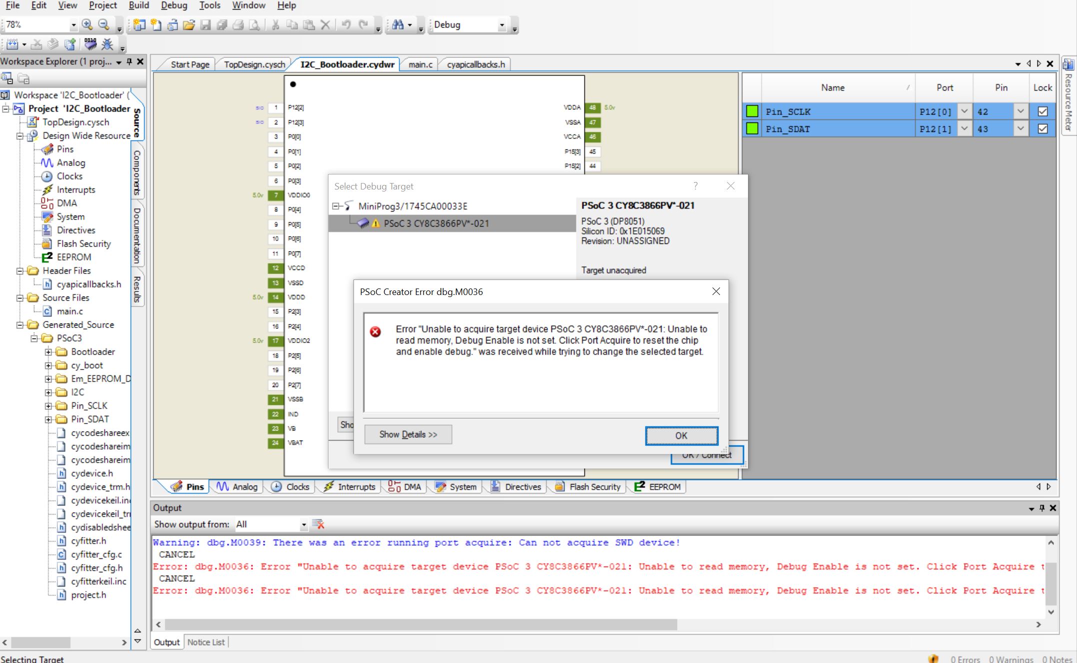
Hello, I recently purchased the CY8C3866PVI-021 and am having trouble getting it programmed. I have the miniprog3 programmer and I made a little developer board for the chip in eagle using the recommended circuit on the datasheet, but every time I try and program the chip I get a yellow triangle that shows up next to the chip after it is identified and I receive the following error on attempted programming "Error "Unable to acquire target device PSoC 3 CY8C3866PV*-021: Unable to read memory, Debug Enable is not set. Click Port Acquire to reset the chip and enable debug." was received while trying to change the selected target." I believe this to be some sort of communication issue. I previously had this chip on an SMD to DIP adapter and wired on a breadboard and I was able to get passed this error, but it erred once it started programming it missed an ACK bit and failed to program. The reason I made this board was because I suspected a communication issue, so I put all the recommended capacitance's and minimal trace distances, but now I'm stuck on the first error I had and cant even get to the programming part. What am I doing wrong here?
- Mark as New
- Bookmark
- Subscribe
- Mute
- Subscribe to RSS Feed
- Permalink
- Report Inappropriate Content
The following information might help: http://www.cypress.com/comment/262701
Also, please attach the screenshot of the port settings, it will be help me debug better. The following KBA lists the scenarios of different errors which occur based on the port settings and might prove useful: Troubleshooting PSoC® 3/4/5LP Programming/Debugging Issues - KBA210619
Do let me know if you face any difficulties.
Regards,
Dheeraj

- Mark as New
- Bookmark
- Subscribe
- Mute
- Subscribe to RSS Feed
- Permalink
- Report Inappropriate Content
Dheeraj,
Here is a screen shot of my settings. I have tried SWD 10 pin and JTAG, I've tried programmer supplied power and externally supplied power, I've tried raising and lowering frequency, I've tried reset mode and power cycle mode. Nothing seems to work. As you can see in my screen shot, the chip is being identified, but it is noted that there is some issue by the yellow warning triangle. I'm thinking this is some communication issue, but I am not sure.
Josiah
- Mark as New
- Bookmark
- Subscribe
- Mute
- Subscribe to RSS Feed
- Permalink
- Report Inappropriate Content
Can you share the schematic of your custom board?
Regards,
Dheeraj
- Mark as New
- Bookmark
- Subscribe
- Mute
- Subscribe to RSS Feed
- Permalink
- Report Inappropriate Content
Dheeraj,
Here is the schematic and board design. I added optional pull up/down resistors and tried the board with and without to see if they help, although the programming manual does not include them and says they are internal. I'm using the datasheet recommended 8K for pullups.
Josiah
- Mark as New
- Bookmark
- Subscribe
- Mute
- Subscribe to RSS Feed
- Permalink
- Report Inappropriate Content
Is it possible for you to share your schematic as a pdf? It will be easier.
Regards,
Dheeraj
- Mark as New
- Bookmark
- Subscribe
- Mute
- Subscribe to RSS Feed
- Permalink
- Report Inappropriate Content
- Mark as New
- Bookmark
- Subscribe
- Mute
- Subscribe to RSS Feed
- Permalink
- Report Inappropriate Content
I reviewed your schematic and these are my observations:
#1: You have 1uF Capacitor (C6) connected between XRES (P1[2]) and P1[1]. If you have added this to filter glitches then it should be of a small value like 0.1uF and it should be connected as shown below:

#2: Pin 36 (VDDD) seems to be connected to ground. It must be connected to power supply.
#3: For Reset mode programming, make sure you have enabled XRES in the DWR window as mentioned in the following KBA:
Programming Modes Supported in a 48-Pin PSoC® 3 Device – KBA94456
#4: Power cycle programming can also be done
With these changes you must be able to acquire the device. Let me know if it works.
Regards,
Dheeraj
- Mark as New
- Bookmark
- Subscribe
- Mute
- Subscribe to RSS Feed
- Permalink
- Report Inappropriate Content
sorry, my schematic is unnecessarily confusing because I did not follow convention for the pin numbering. The numbers on the right are all flipped vertically so what you see as pin 36(Vdd) is actually pin 37(Vss) and what you see as pins 26 and 27 (P1[2] and P1[1]) are actually pins 47 and 46 (Vssa and Vcca) I went by the attached example schematic from the datasheet. I've tried both reset and power cycle programming. I checked and Xres is enabled.
Josiah
- Mark as New
- Bookmark
- Subscribe
- Mute
- Subscribe to RSS Feed
- Permalink
- Report Inappropriate Content
The schematic looks fine now. Just to rule out certain silly scenarios, could you try using a different cable to connect the Miniprog 3 and the PC and then checking if you see the same error?
Regards,
Dheeraj
Cypress Applications Engineer